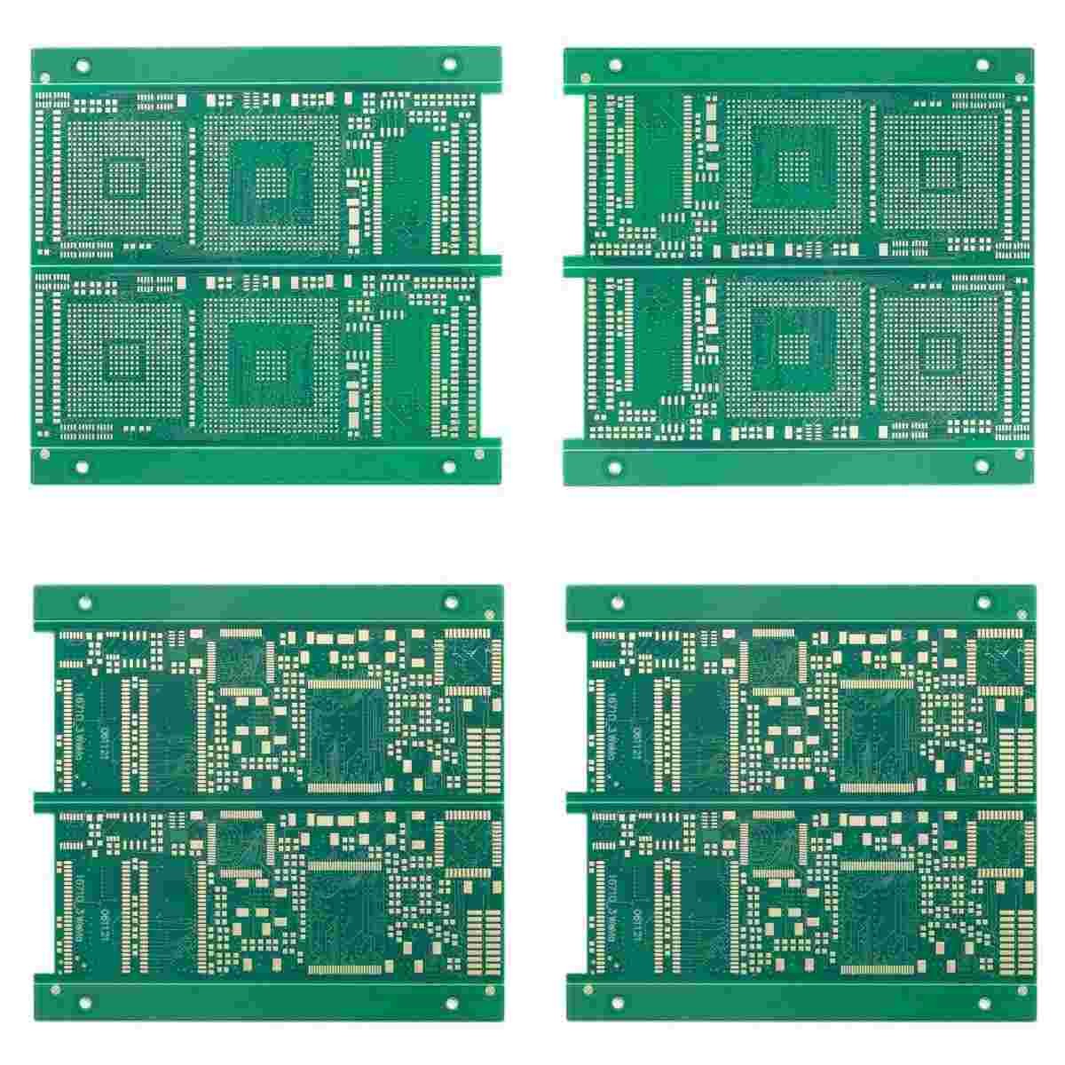
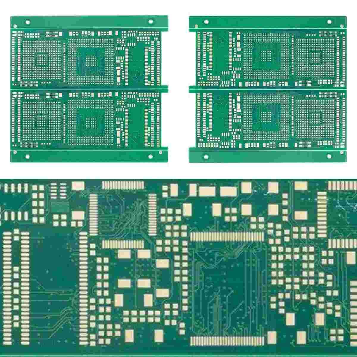
Multilayer HDI PCB Board 0.9mm 8 Layer Pcb Fabrication Green Solder
Mask
HDI PCB Board Multilayer PCB Board 8 Layer PCB Board HDI Board
China PCB Assembly PCB Fabrication Service PCB Assy
8L 2+N+2 HDI Boards
HDI PCB means high density interconnect printed circuit boards,
they are characterized by finer lines, closer spaces, and more
dense wiring.
Due to its higher circuit density than traditional circuit boards,
HDI PCB designs can include smaller through holes and capture pads,
as well as higher connection pad density. HDI PCB is widely used to
reduce the weight and overall dimensions of products, as well as to
enhance the electrical performance of the device.
HDI Board Stack-up:
1+N+1 with laser microvia and mechanical buried core via. The “1”
represents “build-up” or sequential lamination on each side of the
core.
i+N+i (i>=2) PCBs contain 2 or more “build-up” of high-density interconnect
layers. Microvias on different layers can be staggered or stacked.
Copper filled stacked microvia structures are commonly seen in
challenging designs.
| PCB Layer | 8L | PCB material | FR4 TG170 |
| Copper thickness | 1/H/1/1/H/H/H/1 OZ | PCB thickness | 0.9MM |
| Min. hole size | 0.15mm | Min.PCB track/gap: | 3/3mil |
| PCB solder mask | Green | PCB silkscreen | White |
| PCB surface finished | Immersion Gold | PCB outline | Routing/V-CUT |
| Application | industrial control |
| Special requirement: | small line space and gap:3/3mil/HDI Buried vias and blind vias, two
step stack up /min. via hole size 0.15mm/impedance control/resin
filled and plated over/0.25mm BGA |
FAQ:
Q1:Are you a factory or trade company?
A: Yes, we are the factory, we have independent quick turn
prototype PCB manufacturing & big volume PCB production lines.
Q2:What kind of PCB file format can you accept for production?
A: Gerber, PROTEL 99SE, PROTEL DXP, POWER PCB, CAM350, ODB+(.TGZ)
Q3:Are my PCB files safe when I submit them to you for
manufacturing?
A: We respect customer's copyright and will never manufacture PCB
for someone else with your files unless we receive written
permission from your side, nor we'll share these files with any
other 3rd parties. And we could sign NDA with client if necessary.
Q4:If we have no PCB file/Gerber file, only have the PCB sample,can
you produce it for me?
A: Yes,we could help you to clone the PCB. Just send the sample PCB
to us, we could clone the PCB design and work out it.
Q5:What is your standard lead time for PCB?
A: Sample/prototype(less than 3sqm):
1-2 Layers: 3 to 5working days (fastest 24hours for quick turn
services)
4-8 Layers: 7~12 working days (fastest 48hours for quick turn
services)
Mass production (less than 200sqm):
1-2 Layers:7 to 12 working days
4-8 Layers:10 to 15 working days
Q6:What payment do you accept ?
A: Wire Transfer(T/T) or Letter of Credit(L/C) or Paypal(only for
small value less than 500usd)
Q7: What is the shipment way?
For heavy goods more than 300kg, we may ship your PCB boards by
ship or by air to save freight cost. Of course, if you have your
own forwarder, we may contact them for dealing with your shipment.
Q8:What is your minimum order quantity?
A: No MOQ.The quantity will only affect the price. Please contact
us for RFQ.


